|
|
The introduction of nanoelectronics provides two categories of advantages:
Nano
|
- Smaller device size
- Higher device density
- Lower power
- Self-assembly
- Close-coupling of adjacent devices
|
Logic
|
- Complex device characteristic
- Precision appropriate to analog computation
- Higher logic throughput
- Programmable discontinuities
- Compatibility with sensors and molecular electronics
|
Nanoelectronic devices
There is an extensive literature on nanoscale electronic devices. These devices have been developed extensively since the 1980s, and now offer a wide range of functionality with existing technology. They are the object of continuing research and development.
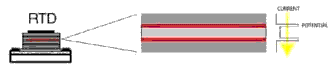
A typical nanoelectronic device is the resonant tunneling diode (RTD), shown in the following diagram. This device consists of multiple nanoscale layers of doped semiconductors, fabricated to generate one or more potential wells. Application of a voltage across the device causes current to flow, but the current is a highly nonlinear function of the voltage due to the quantization of energy levels in the very small structure.
- One-dimensional nanoelectronic devices such as RTDs have a lateral size about that of normal microelectronic devices (about 1 μm2), and can be stacked perhaps 10-100 deep. Each RTD generates roughly a cubic (V3) function, hence 10 of them stacked will generate an order-30 polynomial. Discontinuities in I(V) can be made very localized, and multiple devices can be assembled into a equivalent devices generating a very complex functions. All this complexity is generated within a device about 1 μm3. We can easily envision arrays of these devices connected in series (or rings or any other network). A 1 cm2 chip could easily hold 106 of these devices, quite enough to provide wide versatility in linear computations, and perhaps enough to implement 2D arrays.
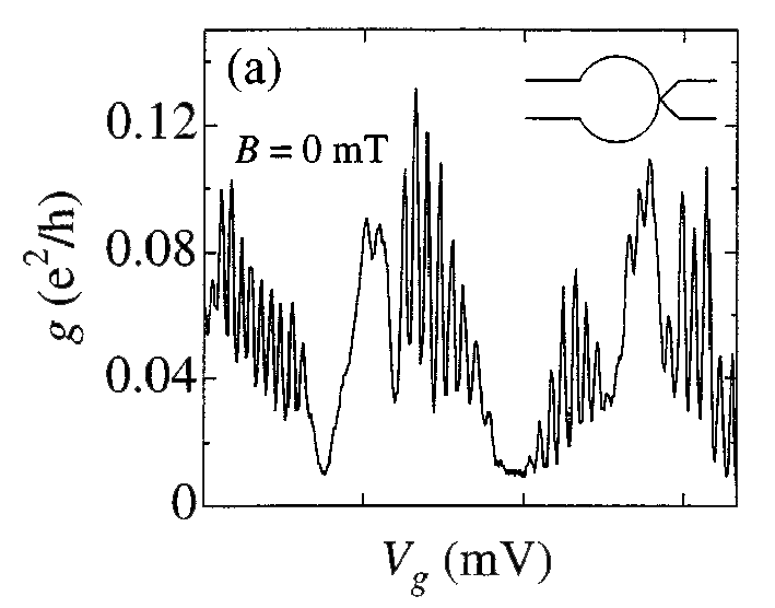
- Besides RTDs, there are many other nanoelectronic device classes that provide many options for generating complex discontinuous functions, including quantum dots, superconducting quantum interference devices (SQUIDs), electrostatic corrals, and single-electron transistors. Many of these devices, including RTDs, can generate multi-peak functions representing a fairly high-order polynomial. Devices that operate using coulomb blocking typically have a periodic I(V) characteristic. The figure below [ S. M. Cronenwett, S. M. Maurer, S. R. Patel, C. M. Marcus, C. I. Duruoz, and J. S. Harris, Phys. Rev. Lett. 81, 5904 (1998)] shows the experimental conductance through a quantum dot, as a function of applied voltage.
This figure should dispel any doubts about whether sufficiently complex functions can be generated with nanoscale devices. Of course, it remains to be demonstrated that a particular desired characteristic can be obtained. We feel secure in assuming that any (reasonable) characteristic of (nearly) arbitrary complexity can be synthesized using nanoscale devices.
- Nanoelectronic circuits
- The behavior of nanoelectronic devices is dominated by quantum effects, which are usually nonlinear. Instead of suppressing such nonlinearities to force such devices to act as simple switches (for digital computing) or as linear amplifiers (for analog computing), we propose to exploit the nonlinearity to provide increased logic density and logic throughput.
The I(V) characteristic of quantum devices can be tailored to be super- or sub-ohmic. RTDs are usually observed to have an N- or S-shaped curve. Combinations of devices, easily achieved by stacking multiple layers, produces compound characteristics that can have many peaks, sometimes resembling a polynomial. Indeed, the engineering is sufficiently advanced that we simply assert that we can produce any characteristic (within a wide but reasonable range). This is the basis for using nanoelectronic devices as function generators, which is tantamount to their use as first-return maps in analog circuits.
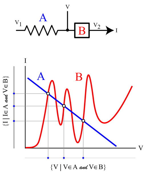
A significant aspect of nonlinear devices is that they can produce discontinuities, including switching. In the simple gate circuit above, the linear resistor characteristic intersects the tri-model RTD characteristic in three stable points (the three other intersections are unstable). The circuit will exist stably in any of these three points; an external stimulus can be used to make the circuit jump from one point to another.
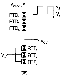
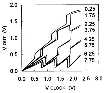
The existence of sharp jumps and discontinuities in nanoelectronic devices is extremely valuable because it enables analog switching. For example, the following figure [T. Waho, "Resonant Tunneling transistor and its Application to Multiple-Valued Logic Circuits," Proc. Conf. Multiple-Valued Logic, IEEE 0-8186-7118-1/95 (1995)] shows a stack of 6 devices that produce 23=8 functions as VG is varied between 0.25 and 7.75 volts.
Nanoelectronics as the technology of choice
The choice of nanoelectronics (rather than, say, CMOS) is largely based on the exceptionally fortuitous match to several aspects:
- Large numbers of devices in regular arrays, which enables partial casting of algorithms into hardware;
- Analog circuits match required and adaptable precision of real-world human-important problems;
- Compound close-coupled devices for generating complex characteristic transfer functions, i.e., higher logic density and throughput.
- While any one aspect may not be a determinant in selecting nanoelectronics, the several factors mentioned above provide compelling evidence, and motivation, for selecting nanoelectronics to implement nanologic.
-
-
|